INUP-i2i
Scope
The scopes of the program are schematically illustrated below.
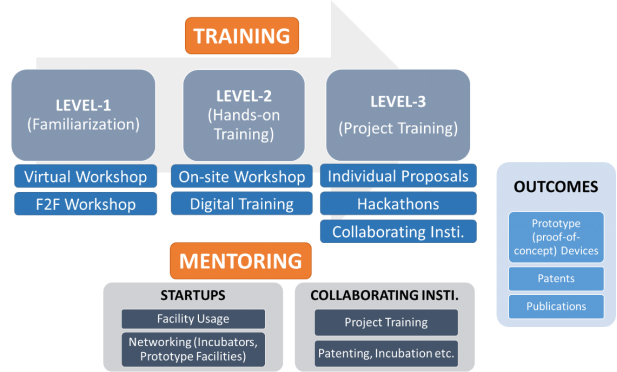
At the Level 1 to start with a large number of aspiring participants with familiarization lectures spanning 2-3 days on diverse areas of nanoscience and nanotech that include, circuits, MEMS cantilever, microfluidics, spintronics, transistors, interdigitated electrode devices, semiconductor LEDs, photovoltaics and nanophotonics, among others.
A section of the Level 1 participants is to be selected into the Level 2 for the hands-on training program wherein 10-15 days of rigorous hands on training to be provided on various basic nanoelectronics devices and protocols.
A section of the Level 2 participants is to be graduated to the Level 3 wherein they will be allowed to submit a proposal to the Nanocenters and execute their proposal for 3 months (short term) and 6 months (medium term).
At the end of the cycle it is expected that the users are able to develop routine nanoelectronics prototypes targeting various applications, develop novel devices, publish in the international journals, patent new ideas and facilitate start-ups. The Nanocentres will also find (i) a host of potential collaborators in order to promote a greater number of participants in the program and facilitate deliverables and (ii) industrial partners for whom trainings can be arranged at these state-of-art facilities.